
Resource-efficient and low-power implementation of the Q-learning algorithm on FPGA
- Published
- Accepted
- Received
- Academic Editor
- Paulo Jorge Coelho
- Subject Areas
- Algorithms and Analysis of Algorithms, Embedded Computing, Optimization Theory and Computation, Real-Time and Embedded Systems, Operating Systems
- Keywords
- Convergence, Hardware accelerator, Low power, FPGA, Optimal policy, Q-learning
- Copyright
- © 2026 S Bazmalah et al.
- Licence
- This is an open access article distributed under the terms of the Creative Commons Attribution License, which permits unrestricted use, distribution, reproduction and adaptation in any medium and for any purpose provided that it is properly attributed. For attribution, the original author(s), title, publication source (PeerJ Computer Science) and either DOI or URL of the article must be cited.
- Cite this article
- 2026. Resource-efficient and low-power implementation of the Q-learning algorithm on FPGA. PeerJ Computer Science 12:e3351 https://doi.org/10.7717/peerj-cs.3351
Abstract
Q-learning (QL) is a reinforcement learning technique. It enables agents to learn optimal policies by iteratively updating action-value functions (Q-values). The deployment of Q-value storage and updating is critical to operational efficacy during training. This article presents a resource-efficient and low-power Q-learning algorithm implementation on field programmable gate arrays (FPGAs) by using a temporary memory to optimize updating Q-values during learning. The design was implemented on a Genesys 2 Kintex7 (XC7K325T-2FFG900C) FPGA. It is analysed for different state scenarios, Q-Matrix sizes, and fixed-point formats. The proposed design achieves convergence to the optimal policy. Compared with the literature, the proposed design with 1,024 states at 16 bits achieves a 71.9% reduction in look up tables (LUTs), a 66.4% reduction in flip-flops (FFs), a 75.6% reduction in block random access memories (BRAMs), and a 67% reduction in power consumption. Similarly, with 1,024 states at 32 bits, it achieves a 73.8% reduction in LUTs, a 65.8% reduction in FFs, a 59.8% reduction in BRAMs, and a 65.7% reduction in power consumption. These significant improvements in resource utilization and power efficiency make the proposed design well-suited to applications that demand efficient and rapid information processing and also require fewer hardware resources.
Introduction
In recent decades, artificial intelligence (AI) and machine learning (ML) techniques have gained much attention due to improvements in computational systems in terms of performance, power, and space. Reinforcement learning (RL) is one category of ML. RL is a trial-and-error learning strategy. It uses feedback to enhance its agent performance (Theobald, 2017), which gets a reward that can be either positive or negative and gradually improves its actions to maximise the collective reward. Figure 1 illustrates the learning process in RL.
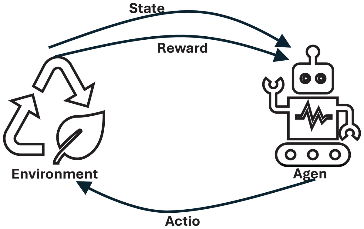
Figure 1: Learning process in reinforcement learning (RL).
Among RL algorithms, deep reinforcement learning (DRL) algorithms, including deep Q-networks (DQN) and proximal policy optimization (PPO), have focused on deep reinforcement learning (DRL) with neural networks. These methods require significant processing power, computational resources, and extensive training time and memory. Such demands limit their practicality in resource-constrained environments that require low latency, efficiency, and predictable performance. Q-learning (QL) provides a lightweight structure that avoids the overhead of neural network training while still ensuring convergence to the optimal policy. This makes Q-learning suitable for resource-limited systems, such as embedded systems.
RL hardware acceleration has been a popular research area (Rothmann & Porrmann, 2022a). Researchers and engineers have been investigating various techniques to improve the efficiency and speed of RL algorithms on specialized hardware platforms. The training process of RL algorithms can be accelerated by utilizing hardware accelerators, such as graphics processing units (GPUs), field-programmable gate arrays (FPGAs), or central processing units (CPUs), that perform computationally expensive operations more efficiently.
Q-learning has successfully resolved complicated sequential decision-making issues. Q-learning is a model-free reinforcement learning method. It has the advantage of evaluating utility and updating control policies without the need for models of the environment (Wei, Liu & Shi, 2015; Al-Tamimi, Lewis & Abu-Khalaf, 2007). Watkins proposed QL in 1989 (Watkins & Dayan, 1992). QL is a value-based and off-policy algorithm. The QL updates the Q-values iteratively at each step (Sewak, 2019) without making any assumptions about the specific policy being applied (Saini, Lata & Sinha, 2022). Implementing Q-learning on FPGAs is particularly beneficial, since FPGAs allow for customized parallel architectures that accelerate Q-value updates and memory operations with reduced power consumption. QL is composed of three elements, which are state, action, and reward combination, called quality or (Q-Value) (Ris-Ala, 2023). The Q-value is calculated using the following equation:
(1) where st and st+1 represent the current and subsequent states of the environment, respectively, similarly, at and at+1 are the current and next actions selected by the agent, respectively. Q(st, at) is the Q-value associated with taking current action at in current state st. The discount factor, γ, lies within the range [0, 1]. Furthermore, α is the learning rate, where , and rt is the current reward value. Finally, QL uses max to select the maximum Q-value among all possible actions for the next state. The QL generates a Q-table to store Q-values, using state-action pairs to index the Q-value. The Q-table contains a matrix of size M × N, called the Q-Matrix, where M is the number of states and N is the number of possible actions. The Q-values for every state and action are updated according to Eq. (1).
In the Q-learning algorithm, action-values (Q-values) are iteratively updated to produce optimal behaviours. The efficient access and updating of these Q-values within a memory structure is critical for the system’s scalability and performance (Mnih et al., 2015). Further, a resource-constrained deployment of Q-learning is impacted by the frequency and speed of updates to Q-values during the learning process (Mnih et al., 2015).
During training, the Q-learning algorithm stores and updates Q-values in a Q-table, which involves frequent memory update operations. These operations consume significant time, power, and hardware resources. Several studies have aimed to lower computing cost and optimize memory access patterns in RL. For instance, Mnih et al. (2015) introduced the DQN, which replaced the Q-table with a neural network to approximate Q-values. However, DQN models typically require significant computational resources, which may not be possible for low-power or edge devices. The authors in Sahoo et al. (2021) stored maximum Q-values in a lookup block for each state, but this strategy resulted in delays and increased storage overhead. Similarly, Meng et al. (2020) used a table to store maximum Q-values, while Rothmann & Porrmann (2022b) divided BRAM blocks for each action.
Another approach proposed by Lin (1991), who introduced experience replays and frame skipping to enhance training efficiency and reduce redundant computations. Zeng, Feng & Yin (2018) explored reduced update policies, selectively updating Q-values based on thresholds in value changes, making memory usage more efficient without affecting convergence in a significant way (Zeng, Feng & Yin, 2018).
This article introduces a method to reduce memory access, hence improve architecture performance in terms of resource usage and power consumption. This can be achieved by avoiding unnecessary write-backs of the Q-values to the memory. The proposed method is evaluated based on speed, hardware resources, and overall effectiveness of the learning process.
This article is organized as follows. The QL architecture design is explained in ‘QL Architecture’. ‘Results and Discussion’ provides details on the evaluation, analysis results, and state-of-the-art architecture, and lastly, ‘Conclusions’ concludes the article.
QL architecture
The architecture for the QL algorithm has been implemented using MATLAB 2020b (The MathWorks, Natick, MA, USA) and Vivado 2020.2. MATLAB and Simulink were utilized to simulate the QL algorithm and develop the overall system design. Xilinx Vivado was employed to synthesize the design for the FPGA. A Grid-World environment has been implemented to evaluate the architecture on the Xilinx Kintex 7.
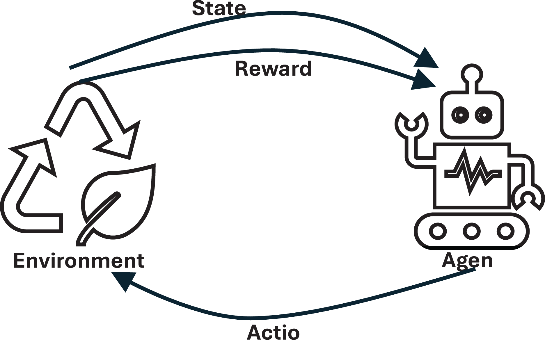
Figure 2 shows the Q-learning architecture implementation on the Kintex 7 XC7K325T-2FFG900C FPGA. The proposed architecture is designed based on a pipeline and parallel structure. Some architectural structures are inspired by the QL hardware accelerator (Meng et al., 2020). The system is designed to work with M states and N actions, resulting in M × N state-action pairs. At the start of each episode, the initial state is chosen randomly, while subsequent states are determined based on the current state and chosen action. Similarly, the first action is selected randomly, while the next action is chosen according to the ε-greedy policy.
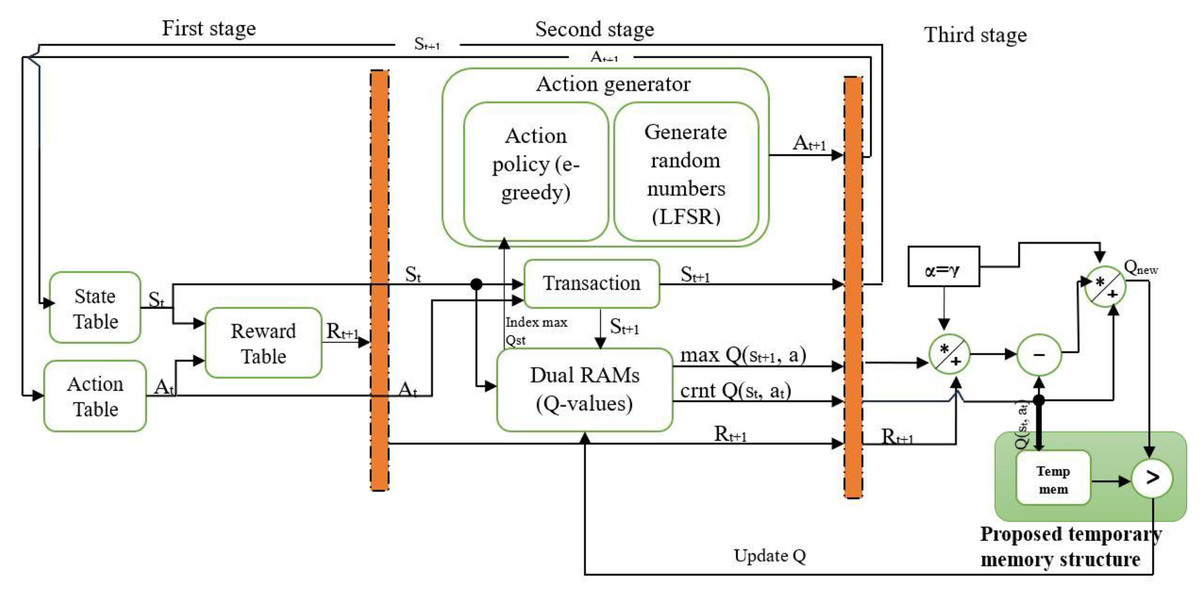
Figure 2: The proposed QL architecture with temporary memory.
In the context of QL, the agent has to balance exploration and exploitation to reach the optimal policy by choosing the best action. Thus, in this work, the action for the next state st+1 is determined based on the ε-greedy policy, which is quite effective in various RL environments (Sutton & Barto, 1998). In the ε-greedy (Langford & Zhang, 2007) policy, the exploration and exploitation are balanced by the parameter ε, where . With a probability of , the action with the highest Q-value is selected (exploitation), while with a probability of ε, the action is chosen randomly (exploration). In this work, different values of the parameter ε were tested. Initially, ε was set to its maximum value of 1 and gradually reduced to 0.00 to identify the optimal setting.
This work used two dual-port RAMs to store the Q-Matrix, which contains all Q-values corresponding to state-action pairs. Dual-port RAM allows for concurrent reading and writing operations, facilitating quick Q-value updates and accelerating learning. It is essential to determine each state-action pair’s current Q-value and the next state’s maximum Q-value for all actions to calculate the Q-value based on Eq. (1). This work used parallel processing to obtain the current Q-value of state-action pairs , the max Q-value of the next state for all actions (Max_Q (st+1, a)), as well as the index of the maximum Q-value of the current state from memory. The key behind finding the index is that it represents the action that can be used by the ε-greedy policy to move from the current state to the next state. All these values were obtained from the first dual-port RAM. The second dual-port RAM was used to find the Q-value of the current state. The maximum Q-value was selected using a MAX logic operation requiring fewer hardware resources. The implementation of parallel processing yields performance improvements and optimizes the overall system. The parallel processing allows current Q, maximum Q, and next action to be calculated at the same time in stage 2. The configuration is shown in Fig. 3. Both hyperparameters, α and γ, were assigned equal values of 0.875. Then, Eq. (1) is applied to calculate the new Q-value .
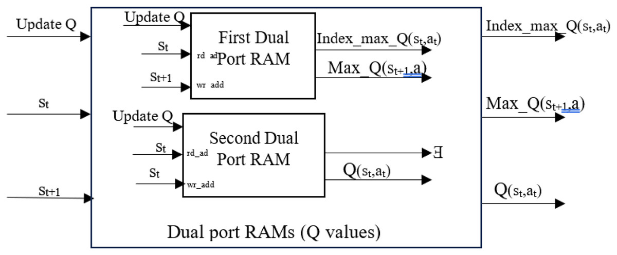
Figure 3: Parallel structure and processing to obtain values.
This work introduces a method for updating Q-values that reduces BRAM usage, thereby lowering resource consumption, power usage, and processing time. A temporary memory was used to store the current Q-value, enabling faster access and avoiding unnecessary reads and writes to BRAM, as shown in the third stage in Fig. 2. Each new Q-value computed during the learning process was compared directly against it, as shown in Fig. 4. A MAX comparison was used to compare and determine whether the new Q-value is larger than the current Q-value in the temporary memory. If the new Q-value is larger, it is written back into dual-port RAMs in the corresponding location; otherwise, the previous value is kept, which means memory access is not required. This is a practical approach that reduces unnecessary memory writes, and only meaningful improvements are stored. This technique can improve hardware resource utilization. It reduces negligible writing operations that would otherwise consume additional power and time, particularly in high-frequency learning environments. Moreover, it facilitates achieving convergence by systematically improving the Q-values.
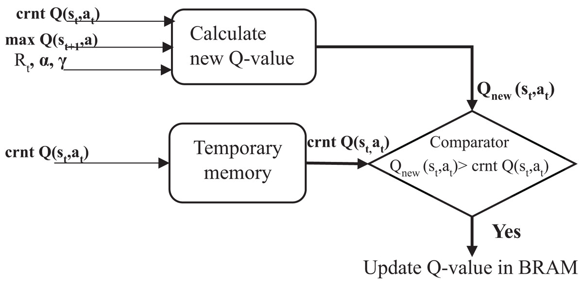
Figure 4: Proposed method structure.
Results and discussion
Analysis of results
The simulation and synthesis analyses various scenarios, each incorporating a different number of states and actions. All scenarios were simulated and synthesized with a fixed-point representation represented as [n, b], where n indicates the number of bits and b shows the number of bits in the binary part in two different scenarios (different word lengths). Fixed-point can enhance performance, and hardware resources can be conserved (Nguyen, Kim & Lee, 2017; Kara et al., 2017). Additionally, fixed-point can be very efficient in FPGA designs (Kara et al., 2017).
Q-value updates, processing times, and throughputs differ in each episode. Thus, the average throughput for each M state was calculated. The throughput is defined as the number (in millions) of Q-values (samples) computed per second (MSPS) (Meng et al., 2020).
In this work, the value of ε is set to 0.01. This value yielded a significant number of actions that were taken through the learning process, as explained in Sutton & Barto (2018). Besides the value of the epsilon parameter, the proposed optimization approach provided optimal results in updating more Q-values. It contributed to enabling faster convergence, and enhancing processing, learning, and throughput.
The presented design architecture requires only three DSPs to calculate the new Q-value. The design was analyzed based on the implementation results for the most critical resources for the FPGA. The implementation results for Kintex 7 XC7K325T-2FFG900C FPGA resources are expressed in terms of look up tables (LUTs), look up table RAMs (LUTRAMs), flip-flops (FFs), and BRAMs. Tables 1 and 2 illustrate the implementation results obtained for all scenarios with four actions in terms of hardware resources and power consumption. Moreover, Tables 3 and 4 illustrate the implementation results obtained for all scenarios with eight actions, detailing hardware resources utilization and power consumption. Also, the percentage usage relative to the total available is provided. As well, it contains the result of throughput in Mega Samples per second in the seventh column (in this work, throughput was calculated as the number of updated Q-values per time) and the maximum clock frequency (CLK) in the eighth column.
| States | LUT | LUTRAM | FF | BRAM | Thr. (MSPS) | CLK MHz | Power (mW) |
|---|---|---|---|---|---|---|---|
| 8 | 543 0.27% | 64 0.10% | 724 0.18% | 0 | 779.8 | 145 | 21 |
| 16 | 560 0.27% | 36 0.06% | 932 0.23% | 1 0.22% | 703.5 | 145 | 28 |
| 32 | 534 0.26% | 37 0.06% | 664 0.16% | 1 0.22% | 604.5 | 145 | 27 |
| 64 | 552 0.27% | 38 0.06% | 669 0.16% | 1.5 0.34% | 816.4 | 190 | 28 |
| 128 | 568 0.28% | 39 0.06% | 684 0.17% | 1.5 0.34% | 802.8 | 190 | 29 |
| 256 | 647 0.32% | 43 0.07% | 696 0.17% | 1.5 0.34% | 540.5 | 190 | 31 |
| 512 | 674 0.33% | 47 0.07% | 987 0.24% | 2.5 0.56% | 444.02 | 190 | 36 |
| 1,024 | 642 0.32% | 47 0.07% | 719 0.18% | 5 1.12% | 437.15 | 190 | 40 |
| States | LUT | LUTRAM | FF | BRAM | Thr. (MSPS) | CLK (MHz) | Power (mW) |
|---|---|---|---|---|---|---|---|
| 8 | 552 0.27% | 48 0.08% | 694 0.17% | 2 0.45% | 874.98 | 100 | 21 |
| 16 | 555 0.27% | 50 0.08% | 706 0.17% | 2 0.45% | 744.98 | 94 | 22 |
| 32 | 593 0.29% | 52 0.08% | 721 0.18% | 2 0.45% | 668.5 | 94 | 23 |
| 64 | 609 0.30% | 54 0.08% | 728 0.18% | 2.5 0.56% | 674 | 73 | 24 |
| 128 | 630 0.31% | 56 0.09% | 740 0.18% | 2.5 0.56% | 559.1 | 94 | 26 |
| 256 | 776 0.38% | 62 0.10% | 1,032 0.25% | 2.5 0.56% | 468.9 | 73 | 28 |
| 512 | 675 0.33% | 60 0.09% | 764 0.19% | 4.5 1.01% | 438.6 | 73 | 30 |
| 1,024 | 706 0.35% | 63 0.10% | 776 0.19% | 9 2.02% | 407.5 | 73 | 36 |
| States | LUT | LUTRAM | FF | BRAM | THR. (MSPS) | CLK (MHz) | PWR (mW) |
|---|---|---|---|---|---|---|---|
| 8 | 623 0.31% | 66 0.10% | 1001 0.25% | 0 | 254.39 | 140 | 25 |
| 16 | 570 0.28% | 33 0.05% | 929 0.23% | 1 0.22% | 156.36 | 140 | 27 |
| 32 | 595 0.29% | 31 0.05% | 940 0.23% | 1.5 0.34% | 157.07 | 140 | 30 |
| 64 | 599 0.29% | 33 0.05% | 942 0.23% | 1.5 0.34% | 115.19 | 140 | 31 |
| 128 | 614 0.30% | 30 0.05% | 941 0.23% | 1.5 0.34% | 201.28 | 140 | 32 |
| 256 | 627 0.31% | 31 0.05% | 945 0.23% | 1.5 0.34% | 390.17 | 140 | 33 |
| 512 | 671 0.33% | 32 0.05% | 947 0.23% | 2 0.45% | 368.13 | 140 | 35 |
| 1,024 | 706 0.35% | 33 0.05% | 953 0.23% | 3.5 0.79% | 360.01 | 140 | 39 |
| States | LUT | LUTRAM | FF | BRAM | Thr. (MSPS) | CLK (MHz) | Power (mW) |
|---|---|---|---|---|---|---|---|
| 8 | 642 0.32% | 49 0.08% | 990 0.24% | 1.5 0.34% | 400 | 80 | 23 |
| 16 | 653 0.32% | 50 0.08% | 993 0.24% | 1.5 0.34% | 700 | 80 | 24 |
| 32 | 660 0.32% | 49 0.08% | 990 0.24% | 2 0.45% | 618 | 90 | 25 |
| 64 | 668 0.33% | 50 0.08% | 993 0.24% | 2 0.45% | 445.6 | 90 | 26 |
| 128 | 684 0.34% | 49 0.08% | 996 0.24% | 2.5 0.56% | 385.8 | 80 | 27 |
| 256 | 691 0.34% | 49 0.08% | 999 0.25% | 2.5 0.56% | 256.9 | 80 | 28 |
| 512 | 735 0.36% | 47 0.07% | 1,002 0.25% | 4.5 1.01% | 283.7 | 70 | 29 |
| 1,024 | 774 0.38% | 49 0.08% | 1,005 0.25% | 9 2.02% | 264.24 | 70 | 31 |
It is observed that an increase in the number of states and an increase in the bit-width lead to an increase in the usage of LUTs, LUTRAMs, FFs, and BRAMs of the FPGA board, as shown in Fig. 5. This is justified due to the increased usage to store reward, states, and state transition matrix tables, as well as an increase in the bit-width, which leads to an increase in the width of Q-values, resulting in increased memory usage to store the Q-Matrix and increased processing time. Furthermore, increasing the number of states and bit length leads to decreased throughputs, as shown in Fig. 6, and requires more time to reach the optimal policy and achieve QL convergence.
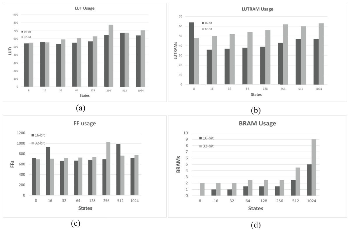
Figure 5: Usage resource for 16-bit and 32-bit architectures across different numbers of states and four actions.
(A) Comparison of LUT consumption. (B) Comparison of LUTRAM consumption. (C) Comparison of FF consumption. (D) Comparison of BRAM consumption.
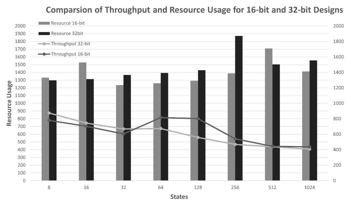
Figure 6: Throughput comparisons of the architecture with different numbers of states and four actions.
A further consideration is the maximum clock frequency. When a certain number of bits and states are used, the clock frequency remains nearly unchanged. This can be explained by the small delay between them. Additionally, when both the number of states increases and the bit length increases, the clock frequency decreases, and a greater effect is observed for 32 bits compared to 16 bits. As a result, an increase in the complexity of the environment leads to an increase in state space, and a greater amount of data needs to be processed. The explanation for this behavior can be found in the growing use of FPGA resources, such as LUTs, FFs, and BRAMs.
Implementing QL with the e-greedy policy, it can face a problem, which is that not all state-action pairs are visited. It means that the agent can get stuck in local optima. In this work, employing the temporary memory facilitates more comprehensive updates to the Q-values and succeeds in visiting most state-action pairs, resulting in achieving convergence quickly.
Power consumption
The eighth column of Tables 1, 2, 3, and 4 shows the dynamic power consumption of the design for each scenario. It is noticed that increasing the number of states and bit lengths leads to increased resource utilization. The 16-bit design requires fewer memory (BRAMs) and registers compared to the 32-bit design, resulting in reduced resource utilization. However, it reveals higher power consumption due to employing higher clock frequencies, as shown in Tables 1 and 3. In contrast, the 32-bit design utilized more resources, which reduced the need for frequent memory access, which is typically a significant power consumer. Thus, power consumption increases significantly when the number of LUTs and BRAMs increases, as illustrated in Fig. 7. As evident from the results in Tables 1, 2, 3, and 4, the proposed design has efficient performance, less resource utilization, and less power consumption, even with increasing bit length.
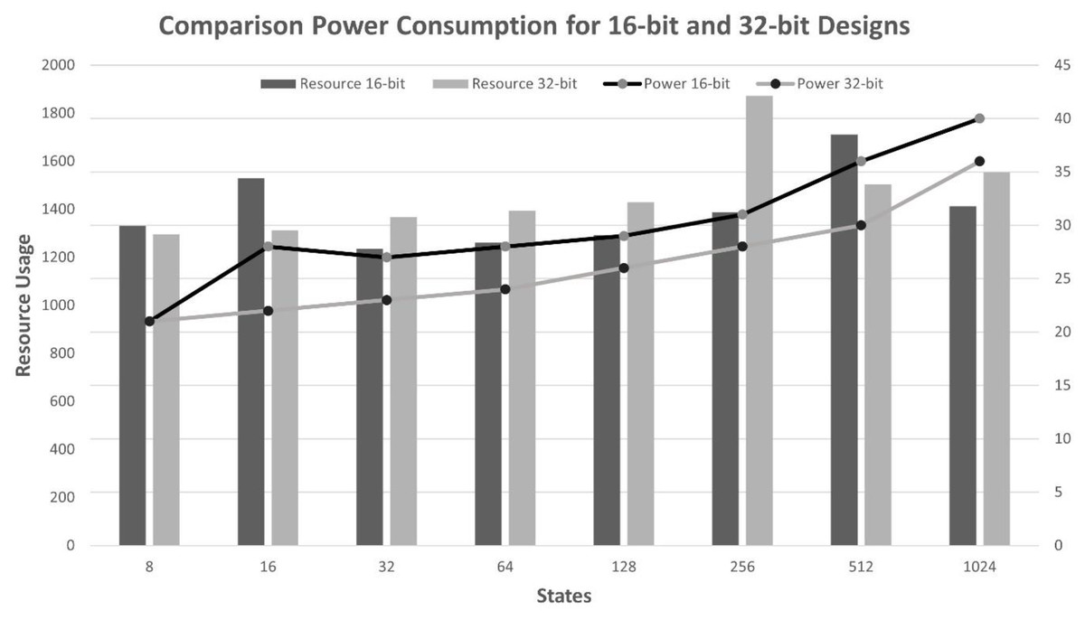
Figure 7: Power comparison of 16-bit and 32-bit designs with four actions.
Comparison of the state of the art
The architecture proposed in this article is compared with a recent Q-learning hardware accelerator architecture presented in Sutisna et al. (2023), which was selected due to its state-of-the-art performance in terms of resource usage and power consumption. The design in Sutisna et al. (2023) was implemented on the Xilinx Virtex UltraScale+ xcvu13p FPGA, which offers a specific set of resources such as LUTs, flip-flops (FFs), BRAMs, and embedded DSPs. To ensure a fair and consistent comparison, the proposed architecture is also synthesized and simulated on the same FPGA device. Although the work in Sutisna et al. (2023) uses an SoC, its architecture is the most similar to the proposed design, enabling an objective evaluation of how the proposed temporary memory enhances performance.
The comparison is conducted against two variants from Sutisna et al. (2023): V1, which employs a parallel architecture, and V2, which utilizes parallel and pipelined architectures. Also, the results were selected that had the same number of states and actions. Table 5 illustrates the comparison between the proposed design and the two methods presented in Sutisna et al. (2023), encompassing the utilization of LUTs, LUTRAMs, FFs, BRAMs, and power consumption.
| Bits | States | Design | LUT | LUTRAM | FF | BRAM | CLK (MHz) |
Power (mW) |
|---|---|---|---|---|---|---|---|---|
| 16 | 512 | V1 (Sutisna et al., 2023) | 2,164 | 20 | 1,930 | 17 | 125 | 72 |
| V2 (Sutisna et al., 2023) | 2,111 | 25 | 2,177 | 20 | 125 | 48 | ||
| This work | 641 | 48 | 959 | 2.5 | 150 | 27 | ||
| 1,024 | V1 (Sutisna et al., 2023) | 2,173 | 20 | 1,932 | 21 | 125 | 82 | |
| V2 (Sutisna et al., 2023) | 2,114 | 25 | 2,178 | 20 | 125 | 52 | ||
| This work | 603 | 46 | 688 | 5 | 130 | 21 | ||
| 32 | 512 | V1 (Sutisna et al., 2023) | 2,690 | 20 | 2,074 | 17 | 125 | 85 |
| V2 (Sutisna et al., 2023) | 2,493 | 24 | 2,350 | 22 | 125 | 68 | ||
| This work | 653 | 60 | 749 | 4.5 | 110 | 41 | ||
| 1,024 | V1 (Sutisna et al., 2023) | 2,675 | 20 | 2,076 | 21 | 125 | 94 | |
| V2 (Sutisna et al., 2023) | 2,497 | 24 | 2,351 | 24 | 125 | 72 | ||
| This work | 677 | 62 | 755 | 9 | 60 | 28 |
The proposed design significantly reduces BRAM usage compared to previous designs by replacing BRAM operations with LUTRAM. As a result, the number of LUTRAMs used is higher. This shift enables a distributed memory architecture, which helps minimize routing delays and enhances processing speed, particularly in parallel and pipelined implementations.
The proposed design consumes less power and fewer FPGA resources compared to both methods V1 and V2 of Sutisna et al. (2023), as shown in Table 5. The proposed design has fewer LUTs compared to V1 and V2. The V1 utilizes 2,173, the V2 utilizes 2,114 at 1,024 states for 16 bits, while the proposed design utilizes 603. Similarly, for the most complex configuration (1,024 at 32 bits), the proposed design has nine BRAMs, while V1 uses 21 and V2 uses 24. Additionally, the proposed design consumes fewer FFs compared to V1 and V2. Further, for throughput, they did not determine the throughput for each state but rather provided 31.11 MSPS for V1 and V2; they achieved 148.55 MSPS and 145.46 MSPS at 16 bits and 32 bits, respectively. Meanwhile, the proposed design achieved various throughputs for different numbers of states at 16 bits and 32 bits, as shown in Tables 1 and 2. The most complex (1,024 for 32 bits) achieved 407.5 MSPS of throughput. Thus, the presented design of this work is more power efficient than those presented in Sutisna et al. (2023).
Clock frequency decreases when the number of states and actions increases, while resource usage and power consumption increase. Even though the clock frequency decreases with an increase in the number of states and actions, the proposed design still achieves low resource usage and power consumption. By reducing both resource utilization and energy requirements, the proposed work enables practical deployment in embedded systems and Internet of Things (IoT) devices, where power and hardware resources are highly constrained.
For completeness, the metrics that can be used to compare are the achieved throughput and speed, as shown in Table 6. The most closed elements (M × N) are chosen. The research in Da Silva, Torquato & Fernandes (2019) showed another FPGA implementation of QL, where the Q matrix has 120 elements. In this case, it achieved a throughput of about 19.67 MSPS. Similar scenarios can be found in Meng et al. (2020) with M = 64 and N = 4 (256 elements) and M = 1,024 and N = 4 (4,096 elements); they achieved 189 MSPS and 187 MSPS, respectively. Meanwhile, the architecture proposed obtained a throughput of about 816.4 MSPS and 437.15 MSPS, i.e., speedup about 4.3× and 2.3×, respectively. Likewise, the work in Spanò et al. (2019) achieved 156 MSPS of throughput at M = 256 and N = 4 for 16 and 110 MSPS of throughput at M = 256 and N = 4 for 32. Conversely, the present achieved 540.5 MSPS and 468.9 MSPS of throughputs, respectively. Table 6 shows the speed-up comparison achieved by this work with the strategies presented in Da Silva, Torquato & Fernandes (2019), Meng et al. (2020), and Spanò et al. (2019). The accelerator presented in this article has a higher speedup than those references.
| Reference | Q-matrix (M × N) | CLK (MHz) | Throughput (MSPS) | Proposed throughput (MSPS) | Speed-up |
|---|---|---|---|---|---|
| Da Silva, Torquato & Fernandes (2019) | 120 | 19.67 | 19.67 | 802.8 | 40.8× |
| Meng et al. (2020) | 64 * 4 | No information | 189 | 816.4 | 4.3× |
| Meng et al. (2020) | 1,024 * 4 | No information | 187 | 437.15 | 2.3× |
| Spanò et al. (2019) | 256 * 4, 16 | 156 | 156 | 540.5 | 3.5× |
| Spanò et al. (2019) | 256 * 4, 32 | 110 | 110 | 468.9 | 4.3× |
The proposed architecture is well-suited for applications that need many states or actions, as well as those that prioritize efficient resource utilization and rapid information processing. Based on the design results, the presented architecture of the implemented QL is fast, has fewer resources, high throughput, low processing time, and low power.
Conclusions
Q-learning is an RL algorithm that can obtain an optimal policy by interacting with the environment without requiring any prior knowledge of the system model. This work proposes a temporary memory to minimize memory access for updating Q-values. This method reduces processing time and enables faster convergence. This results in much higher throughput, requiring fewer resources, and consuming less power. Furthermore, this design achieves an optimal policy with an epsilon value of 0.01, demonstrating better performance compared to previous works. Additionally, the architecture of this work has been compared with the current literature on the state of the art. The optimization method in this article significantly improves performance and successfully reduces processing time. It improved speed by 4.3× and achieved 816.4 MSPS throughput over prior works. Also, the design results demonstrate that it can implement a fast QL accelerator.